Saturday, December 28, 2019

0000 0000 0001 1011

CD4069 CMOS Hex Inverter

What to do when your signal comes out reversed from what you need? If it is only one problem signal, then you could whip up a transistor-based solution as per this useful website. If you need seven signals inverted because of an ordering mishap, then a hex inverter (plus a single transistor solution) might be a better approach.

An inverter is a common logic gate (NOT gate) which has the following symbol and truth table.


If you clump a few NOT gates together in a logic chip - you get a CD4069 hex inverter (see screenshot from the datasheet below). So a "1" or "HIGH" sent to pin 1 (A) returns a "0" or "LOW" on pin 2 (G=Ā), and vice versa.


Fortunately in the many buckets of bits I have a few CD4069UBE chips lying around looking for a purpose. The pinout is very straight forward, but before I use the whole chip to reverse a bunch of signals (next blog), I will test it on a very simple circuit - involving of course a blinking LED.


The 555 is not really disembodied out to the side, but it is just shown here providing a clock signal which is a "1, 0" square wave at a particular frequency. And to show that all of the inputs/outputs are ready for quality inverting, I've plugged all six in plus an extra transistor NOT gate - but why seven? Well, next time I'll look at "fixing" a seven segment display gone slight awry.


Saturday, December 21, 2019

0000 0000 0001 1010

Your own PCB (Part IV)

Now that the 555 signal generator circuit has been designed and tested, the next step is to arrange all of the components on a PCB and hit the manufacture button (oh, and pay!). There are heaps of options but there are just two important ones for me that I'll mention - a copper ground layer (which I always add to my PCBs now that I know how to do it) and panelising the design to maximise the number of PCBs for the price paid.

I like to use a local autorouter, but hard core designers will lay down all the tracks as well - more power to them. My early efforts at manual routing took a lot of time, and although it was a good learning exercise I now just go straight to the autorouter running locally. Fast and accurate!

Try not to stress too much about the design as I don't think I've yet ordered a PCB that I've been entirely happy with - there will always be a detail or two that you don't like and will need to change. Some of my PCBs are on their fifth or sixth iteration and I'm still unhappy! Keep experimenting with the design and take a few days and a few revisits before you hit the "order" button.

I laid out this circuit on a board four times then had it manufactured, noting when it arrived that the connection between pin 6 and the potentiometer had not been made! I can still use the boards (after a quick solder), but this video is about version 5 which I hope has everything ironed out.

Here is a quick video of the 555 signal generator (V5) being laid out.


If you want to make/modify this project, you will find all of the files zipped up and available through this link.

When the PCBs arrive I will solder up the resulting PCB and run it through it's paces.


Saturday, December 14, 2019

0000 0000 0001 1001

Your own PCB (part III)

Once the prototyping and testing for the 555 timer based signal generator is complete, it is time to choose the preferred software to design the PCB and output Gerber files for manufacturing. I've tried a few different options including KiCad and Eagle PCB, but have gone back repeatedly to EasyEDA which works for me. I have made a lot of mistakes on this software - but after a few trials it is a pretty simple interface to use.

There are some great video tutorials online so I am not going to do a step by step build of the circuit. If you really need that support, try the following:

  1. Great Scott "From Idea to Schematic to PCB - How to do it easily!"
  2. Mick Make "#184 Making a PCB using EasyEDA. // Review"
  3. Electronoobs "EasyEDA Full TUTORIAL + Create Component + TIPS"
  4. Julian Illet "I Designed a Printed Circuit Board (PCB)"
  5. EasyEDA documents

For this post, I'm just going to show the EasyEDA interface with the components which are required for the 555 signal generator as discussed in "Your own PCB (part II)".

Next time I'll build the PCB online then after checking I'll submit it for manufacturing.


Saturday, December 7, 2019

0000 0000 0001 1000

Your own PCB (part II)

From time to time I'd like access to a variable square wave generator. For instance when (if?) some non-fake CD4026 chips turn up, they will need a clock signal. I have made a few hobby type circuits based on the 555 timer before and as it's such a familiar and venerable concept that I'd thought it would make the perfect circuit to convert to a bona fide manufactured PCB to show the ease of the process (once you know what you are doing!).

Firstly I cast around for a suitable variant. I really like the look of the circuit on a youtube video called "NE555 Signal Generator Tutorial PCB - 10 Hz to 10 KHz" from user "Electronics Projects - Stefano91ste". The video description generously includes links to the "gerber files" needed to make the PCB. I nearly pressed the button for JLCPCB to make them, but then thought that a smaller smd version might be more suitable for me - plus I can "panelize" the process and have quite a few made, maybe for some of my students.


The large through hole original version
I started right from scratch and looked at a few resources describing how the timer produces the signal. Using this very cool website I played around a bit with the numbers to convince myself I could make a generator that produces a square signal from about 0.2Hz (2.5 seconds on, 2.5 seconds off) to about 1.5KHz. In fact by swapping out the resistors and capacitors R1, R2 and C the possibilities expand considerably. Let's check out a few by first calculating and then building circuits based on the diagram in the video.


The variable pot and switchable capacitors give flexibility
So I'll use the circuit shown below, where different values of the capacitance C in an SMD format are switched in and out along with variation of R2 using a 500kΩ potentiometer:


The next step is to make a prototype and test the calculated output of the circuit.

C1 (nF) R1 (Ω) R2 fixed (Ω) R2 variable (Ω) R2 total Calculated f (Hz) Measured f (Hz)
100.3 9959 9967 470000 479967 14.8 14.4
100.3 9959 9967 0 9967 480.3 477.0
9.685 9959 9967 470000 479967 153.3 149.0
9.685 9959 9967 0 9967 4973.9 5025.0
1.038 9959 9967 470000 479967 1430.3 1385.0
1.038 9959 9967 0 9967 46408.3 43950.0

The output frequency expected was calculated in a spreadsheet using the following formula:


So with the values soldered into the rig shown below I have been able to vary the signal output from about 15Hz to nearly 5kHz. I can go higher or lower if needed by changing the values of R1, R2 and C.


The test rig on a SMD to DIP adapter

Measuring the output signal using a DSO138
In general the circuit works great - each capacitor/resistor combination is slightly "out" from calculated values, but of course the resultant signal can be adjusted using the potentiometer shown. I think the slight errors shown result from a combination of the cheap oscilloscope and the fact that all of these components including wires and breadboard have their own capacitance and impedance.

I'm happy that the proof of concept is now complete - next I will design the PCB online and then move closer to fabrication.


Saturday, November 30, 2019

0000 0000 0001 0111

Your own PCB

So far most of the circuits on this blog have been whipped up on a breadboard or a generic PCB. The solar joule thief showed a PCB which looked a bit more professional, but how does that process actually happen? 

Well, I think I've made most of the mistakes possible and some of my earlier efforts with PCBWAY and JLCPCB were quite comical. It might be worth listing the steps and the gotchas that can crop up along the path to your own PCB.

1. Design your circuit on paper. Use a calculator to check some of the voltages and current in the wires. Later when you look at track widths and separation this might come in handy.


2. Test your circuit using appropriate simulator software if you're up for it - it does take an investment in time. I think it's worthwhile before you fry stuff to have a look at the circuit in a simulator. This is particularly useful if you are experimenting with standard components such as the 555 timer (e.g. as I did here using TinkerCad circuits) or perhaps for checking the flow of logic before wiring the myriad of connections (e.g. as I did here using logic.ly).

3. Breadboard the circuit paying close attention to the voltage and current requirements of your components. In this regard you should at least glance at the datasheets of the components you have chosen! For instance if you are using an LM317 voltage regulator (as I did here), then download and look at the limits shown on the datasheet. Don't ignore decoupling capacitors - these little beauties (generally I use a combination of 47uF and 100nF) smooth out the supply and can make a huge difference to the stability of your circuit. Look carefully at the pinouts - correct orientation of the pins can save you a few fried components. As an example, you may have been making a few projects over the years using the Attiny13 as shown here:


Flushed with success you might then migrate the project to the newer Attiny202 with very different pinouts as follows:


For some reason VCC and GND have moved - which if you're not careful could result in some fried chips!

4. Open up EasyEDA and place your components as required. This blog isn't about how to use this software, and in fact I've used KiCad and Eagle to do the same thing - so choose your weapon! The main consideration is that your software produces what is known as a Gerber file (usually a zip of many files) which describes the PCB in a standard format.

EasyEDA and connecting up your components
EasyEDA placing components on the board
Clicking Gerber, check DRC and head over to manufacturing at JLCPCB
It took me quite a few times to understand what a "ground plane" is and how it can be useful. My advice is to definitely use this feature of PCB design. I learned from watching MickMake and reading a lot of online tutorials. Here is a very quick video showing the addition of a ground plane to a PCB - this was something that I struggled with for a long time.


5. When you are in the JLCPCB site, one definite selection should be to panelise (if you're searching online try "panelize") your board. Before I knew about this feature on JLCPCB, I might spend $18 on 10 boards (which sounds great), instead of panelising and spending $18 on 120 boards - big difference! I learned about panelising from this youtube video which also explains the whole process - what a revelation. If you want a more in-depth explanation, Great Scott has an awesome video here.


To illustrate the whole process I will make a PCB over the next few weeks on this blog. I think I'll use a 555 signal generator as the premise for a few reasons.

Firstly, who doesn't love the 555? It's a good starting point, pretty robust and the central character in a lot of useful circuits. Secondly, from time to time you need a quick reliable clock - for example when making a flashing display - as so many chips rely on a clock signal. Thirdly, there are a lot of example 555 timer circuits out there on the interwebs, so not much time will need to be devoted to actual design and then we can concentrate on the production of the PCB.


Saturday, November 23, 2019

0000 0000 0001 0110

Counting the cost (74HC595 Shift Register...again...)

This week was supposed to be all about the most marvelous CD4026 chip, which I was going to use to count numbers outputting to a 7-segment display. The old favourite 555 timer (of course) was going to be on "clock" duties. But a funny thing happened on the way from China - the CD4026s arrived and had a sudden attack of being completely FAKE!!

To be honest I'm a little shocked because I have enjoyed such success with Chinese companies that it hurts when they send dodgy stuff (hurts them I mean). To rub salt into the wound it was the second lot of fake chips I received this week - the others being LM338 voltage regulators.

I'm getting my money back from AliExpress (hopefully - although they are good with their refund policy), but what I really would like back are the hours and hours of testing and trying to debug circuits which were never going to work in the first instance because of the fakery. Note to self (and anyone else watching) - never buy chips from Si Tai&SH IC accessories Store (CD4026) or shenzhen IC store (LM338). Shame on those guys.

So I've shelved the CD4026 blog for a later date (I have more chips on their way from a different source), and in the meantime and only because I'm so welded to the idea of a 7-segment counter I dragged out an old project which uses the Attiny13a microcontroller and a 74HC595 shift register to "fake" my own version of my own blog (the plot gets real thick about now).

As we've seen before the Attiny13 counts real well, and it also pumps out all the data needed to make the shift register drive not just LEDs but also in this case the patterns required for a 7-segment display (in this case common anode) to count hexidecimally from 0..F.

Here is the circuit:


And of course the Attiny13 needs a little code:


#include <avr/pgmspace.h>     // for reading the progmem values

#define DATA  (1<<PB0)        // pin 5
#define LATCH (1<<PB1)        // pin 6
#define CLOCK (1<<PB2)        // pin 7

// digit patterns for a 7-segment display
const PROGMEM uint8_t digit_pattern[17] =
{
  ~0b00111111,  // 0
  ~0b00000110,  // 1
  ~0b01011011,  // 2
  ~0b01001111,  // 3
  ~0b01100110,  // 4
  ~0b01101101,  // 5
  ~0b01111101,  // 6
  ~0b00000111,  // 7
  ~0b01111111,  // 8
  ~0b01101111,  // 9
  ~0b01110111,  // A
  ~0b01111100,  // b
  ~0b00111001,  // C
  ~0b01011110,  // d
  ~0b01111001,  // E
  ~0b01110001,  // F
  ~0b00000000   // quiet please
  
};

void setup() {

    DDRB = 0b00000111;  // set control pins as output
    PORTB = 0b00000000; // but be quiet to start with
    delay(10);
}

void shiftOut(uint8_t val)
{

    for(uint8_t i=0; i<8; i++) {

        if(val & 0b10000000) {
            PORTB |= DATA;
        }
        else {
            PORTB &= ~DATA;
        }
        // pulse the clock
        PORTB |= CLOCK;
        PORTB &= ~CLOCK;
       val<<=1; // move next bit
    }

    PORTB |= LATCH;
    PORTB &= ~LATCH;

}

void loop() {
        for(uint8_t msg=0; msg<17; msg++) {
            shiftOut(pgm_read_byte(&digit_pattern[msg]));
            _delay_ms(500);
        }
            _delay_ms(500); // extra delay before repeating cycle
}


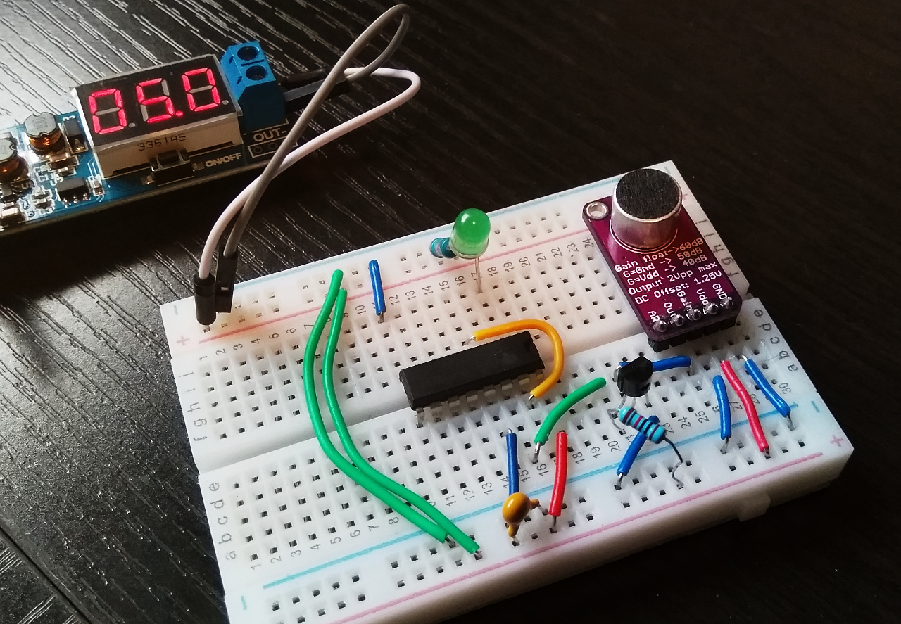
Which just leaves us to breadboard the whole thing up and turn it on:


Saturday, November 16, 2019

0000 0000 0001 0101

Putting some bits and pieces together

So what's the point of a voltage regulator, a police light at 12V, a one touch switch at 6V, an isolating optocoupler, a Darlington Transistor and a police siren (also at 6V)?

Well, you could put them all together in one symphonic circuit to simulate a regular Saturday night in town. You see the flashing lights first - you think they're for someone else - then the siren starts!

I had an idea to use only a single power source for the whole circuit. The maximum voltage needed is 12V (makes sense - it's police car voltage!) but the one touch switch and the siren both need only 6V. Hence I used the LM317 regulator with a 220Ω resistor and a 1kΩ potentiometer set at 836Ω to give the required voltage.

https://circuitdigest.com/calculators/lm317-resistor-voltage-calculator

From the little breadboard with the LM317 the power splits off with 12V going to the police light board and 6V travelling to the one touch switch. The switch output does not have the power to drive the siren which seems to need anywhere from about 160mA to 240mA depending on the frequency of the output. I tried some transistor options but they weren't initially cooperating and instead of creating a new paradigm I thought why not use an optocoupler instead of the LED from the original switch circuit? It would make sense to have the optocoupler on a whole new circuit, isolated from the switch, but I thought seeing as how the whole circuit was based on a simulation, why not simulate the isolation! Er...and laziness.

Sadly the output from the optocoupler (50mA) wasn't sufficient to drive the siren, so I popped in a BC547 (110mA and hFE 200) which allowed a few stuttering pops and splutters from the siren, but not enough to scare any potential perps! 

Then the trusty favourite SS8050 (1.5A and hFE 200) swung into action forthwith which allowed a recognisable but slightly anaemic siren. Finally I remembered the wonders of Darlington Transistors and referred back to the ULN2083 Darlington Array from an earlier blog. Using a whole array on a tiny breadboard seemed a bit over the top so I settled on a TIP120 single Darlington transistor which allows 5A at a hFE of around 2500. Presto we have lights and a switchable siren. Pay no attention to the rogue transistor on the latching switch breadboard with the single blue jumper lead attached to ground - clearly I was trying a few options and forgot to "switch" it out again!


Saturday, November 9, 2019

0000 0000 0001 0100

Two NE555 timers - Police Siren

Inspired by the law enforcement circuit from last week (and with a truckload of 555s available), I looked about for a Police Siren to match the Police Lights. There are seven trillion such circuits out there, but I loved the simplicity and the wonderfully simple instructions found in this video (screenshot below).


https://youtu.be/zDMOsEDxPOc
So off to TinkerCad to make and test the circuit.


Then I built it on a breadboard and here is the siren in all it's screaming glory.


Saturday, November 2, 2019

0000 0000 0001 0011

Two NE555 timers - Police Lights

What could possibly be better than one NE555 timer? Well, maybe you could hook up two of them working together and get some law enforcement action!

Yep, I went looking for a "Police Light" simulator and as usual found many great circuit examples. I liked that this version only contained the 555 (albeit two of) and also it seemed to be a good simulation of the real thing.


The circuit was very simple to make firstly by simulating the lights using Tinkercad Circuits.


Then I made the real thing - works a treat!


Saturday, October 26, 2019

0000 0000 0001 0010

Push on Push off latching transistor circuit

Wouldn't it be nice to not have to have two buttons to switch on and then switch off or reset a circuit? So then you could use just one momentary button and when you push it the circuit turns on, and then pushing it again turns the circuit off. It's like getting something for nothing!

I really do not know why I am fascinated by these types of circuit, the pragmatist in me says that using a latching button or a microcontroller with an interrupt and a few lines of code would be way more practical and way less time consuming (er, and cheaper).

Anyway, after literally hours of searching online I built a couple of circuits which DID NOT work as advertised. They looked dodgy on either youtube or some ad-filled nonsense website and there was little or no explanation for the theory behind the circuits. Finally I found exactly what I was looking for on this wonderful website.

Not only did they have a working circuit diagram, but also a great explanation of all the reasoning behind why it worked - educational!


© https://www.edn.com/


Saturday, October 19, 2019

0000 0000 0001 0001

Attiny13 microcontroller

A little divergence here because it is important to point out that a lot of the logic chips and other components used so far in this blog can easily be replaced by a simple microcontroller. Take for example the CD4017 featured in a previous blog as a clap switch circuit.

Here it the circuit repeated but with the Attiny13 doing the work.


The CD4017 comes in to Aus at around 11c each and the Attiny13 at around 40c each. However the Attiny13 has a great deal of flexibility and in fact programming it to "listen" to sound and then react accordingly is quite straight forward.


#define ledPin PB0
#define TINY_ADC_PB4 0x02
int sensorValue = 0;
int background = 0;
boolean lightup = false;
int sensitivity = 50;     // adjust up for less sensitivity

void setup() {
  pinMode(ledPin, OUTPUT);
  pinMode(TINY_ADC_PB4, INPUT);
  delay(50);
  // take 5 readings and average for background noise
  for (byte i = 0; i < 5; i++) {
    digitalWrite(ledPin, HIGH);
    background = background + analogRead(TINY_ADC_PB4);
    delay(100);
    digitalWrite(ledPin, LOW);
    delay(100);
  }
  background = background / 5;
}

void loop() {

  sensorValue = analogRead(TINY_ADC_PB4);       // take initial reading
  sensorValue = abs(background - sensorValue);  // adjust for background noise

  if (sensorValue > sensitivity) {              // did I hear a clap?

    if (!lightup) {
      lightup = true;
      digitalWrite(ledPin, HIGH);
    }
    else {
      lightup = false;
      digitalWrite(ledPin, LOW);
    }
    delay(50);
  }
  delay(50);
}


Another great advantage of most of these types of microcontroller is that they can be put to sleep and have very little power requirements until required (e.g. woken up with a sensor). That makes them great for battery driven or solar powered projects where energy consumption is an important consideration for design.

One criticism of the Attiny13 microcontroller is lack of memory (only 1k flash!) for larger projects but if you can learn some assembler along with your c-style arduino code, then you can squeeze an awful lot of instructions into it's "tiny", but very capable, brain. Also, I have been known to scale up to the Attiny85 (four times the capacity) or the Atmega series if more features and/or GPIOs are required.

More often than not a combination of parts are required for a particular application, but in general I do reach for a microcontroller first.


Saturday, October 12, 2019

0000 0000 0001 0000

CD4017 counter

The CD4017 is a decade counter and there are a billion or so circuits based on a 555 timer feeding into the counter with the output being a lovely array of LEDs lighting up in response (think KnightRider). Halfway through breadboarding the circuit I came over all bored and went looking for something else to do with the IC. Scrolling down the list of possibilities on a search for alternatives I chanced on a "clap switch" which looked pretty cool.

After building the circuit it soon became evident that you had to be a champion clapper to make it work. I mean what's the point of a clapper circuit if you have to be right next to the microphone and clap like a demon to activate it - you might as well just lean over and flick a switch!

What followed was a few hours of happy transistor swapping. Firstly I tried four (!) SS8050 NPN transistors wired cascade style to increase the gain. It was (only slightly) better but I still got sore hands from clapping. Each SS8050 has a Hfe around 250-300 so I swapped out to a BC517 darlington which jumped up to a ridiculous Hfe around 25k - and it seemed no better as a clap switch.

It occurred to me based on a previous experience with electret microphones to swap out the 100k resistor recommended in the circuit diagram for a trimpot and fiddle with the resistance to affect the sensitivity or gain of the sensor.

At a resistance of around 20k the rig was working pretty well, but as a card carrying perfectionist I then changed out the standard electret microphone for a fancier model which includes it's own crude gain control and voilà, a stupid clap switch.


Saturday, October 5, 2019

0000 0000 0000 1111

LM386 Operational Amplifier

Audio amplifiers come in all shapes, sizes and specifications. We have quite a few different chips in the buckets of components which will see the light of day on this blog. But the very first audio amplifier I built from scratch on a breadboard featured the venerable LM386 opAmp which has been fueling hobbyist dreams since 1969.

I only half read the datasheet (??) so I fed it 27V and popped a few before I realised that I was way over voltage. Fortunately they come in for about AU11c each so it was no big deal to blow a few up in the interests of science?

After a bit more digging around I was able to obtain the LM386N-4 which according to the datasheet should make the most noise.


There are a billion examples of this circuit out there in cyber-world, but I returned a few times to this page and the circuit shown below (which is simple and works well).


This site has such a great tutorial and you can keep adding components to make the sound louder and sweeter. I recommend that if you're serious about these audio amp circuits you head over to the site rather than look at my efforts as I'm only trying to look at how these opAmps might be used. As the original IC was designed for use in an automobile as part of a fuel injection system there might be a few more blogs on this site with this component in other guises.

In the meantime, this is the circuit that I decided to build (with the swap out of 12V for 9V and the LM386N-4 for the standard LM386 opAmp).


If you're unhappy with the sound quality of the amplifier in the video below, remember it's coming through a cheap old speaker and then into a cheap phone microphone. It sounds better in the real world and in fact it has been chugging away on the kitchen bench providing background music for the last few days.