Saturday, December 28, 2019

0000 0000 0001 1011

CD4069 CMOS Hex Inverter

What to do when your signal comes out reversed from what you need? If it is only one problem signal, then you could whip up a transistor-based solution as per this useful website. If you need seven signals inverted because of an ordering mishap, then a hex inverter (plus a single transistor solution) might be a better approach.

An inverter is a common logic gate (NOT gate) which has the following symbol and truth table.


If you clump a few NOT gates together in a logic chip - you get a CD4069 hex inverter (see screenshot from the datasheet below). So a "1" or "HIGH" sent to pin 1 (A) returns a "0" or "LOW" on pin 2 (G=Ā), and vice versa.


Fortunately in the many buckets of bits I have a few CD4069UBE chips lying around looking for a purpose. The pinout is very straight forward, but before I use the whole chip to reverse a bunch of signals (next blog), I will test it on a very simple circuit - involving of course a blinking LED.


The 555 is not really disembodied out to the side, but it is just shown here providing a clock signal which is a "1, 0" square wave at a particular frequency. And to show that all of the inputs/outputs are ready for quality inverting, I've plugged all six in plus an extra transistor NOT gate - but why seven? Well, next time I'll look at "fixing" a seven segment display gone slight awry.


Saturday, December 21, 2019

0000 0000 0001 1010

Your own PCB (Part IV)

Now that the 555 signal generator circuit has been designed and tested, the next step is to arrange all of the components on a PCB and hit the manufacture button (oh, and pay!). There are heaps of options but there are just two important ones for me that I'll mention - a copper ground layer (which I always add to my PCBs now that I know how to do it) and panelising the design to maximise the number of PCBs for the price paid.

I like to use a local autorouter, but hard core designers will lay down all the tracks as well - more power to them. My early efforts at manual routing took a lot of time, and although it was a good learning exercise I now just go straight to the autorouter running locally. Fast and accurate!

Try not to stress too much about the design as I don't think I've yet ordered a PCB that I've been entirely happy with - there will always be a detail or two that you don't like and will need to change. Some of my PCBs are on their fifth or sixth iteration and I'm still unhappy! Keep experimenting with the design and take a few days and a few revisits before you hit the "order" button.

I laid out this circuit on a board four times then had it manufactured, noting when it arrived that the connection between pin 6 and the potentiometer had not been made! I can still use the boards (after a quick solder), but this video is about version 5 which I hope has everything ironed out.

Here is a quick video of the 555 signal generator (V5) being laid out.


If you want to make/modify this project, you will find all of the files zipped up and available through this link.

When the PCBs arrive I will solder up the resulting PCB and run it through it's paces.


Saturday, December 14, 2019

0000 0000 0001 1001

Your own PCB (part III)

Once the prototyping and testing for the 555 timer based signal generator is complete, it is time to choose the preferred software to design the PCB and output Gerber files for manufacturing. I've tried a few different options including KiCad and Eagle PCB, but have gone back repeatedly to EasyEDA which works for me. I have made a lot of mistakes on this software - but after a few trials it is a pretty simple interface to use.

There are some great video tutorials online so I am not going to do a step by step build of the circuit. If you really need that support, try the following:

  1. Great Scott "From Idea to Schematic to PCB - How to do it easily!"
  2. Mick Make "#184 Making a PCB using EasyEDA. // Review"
  3. Electronoobs "EasyEDA Full TUTORIAL + Create Component + TIPS"
  4. Julian Illet "I Designed a Printed Circuit Board (PCB)"
  5. EasyEDA documents

For this post, I'm just going to show the EasyEDA interface with the components which are required for the 555 signal generator as discussed in "Your own PCB (part II)".

Next time I'll build the PCB online then after checking I'll submit it for manufacturing.


Saturday, December 7, 2019

0000 0000 0001 1000

Your own PCB (part II)

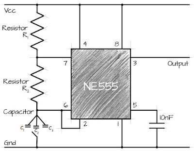
From time to time I'd like access to a variable square wave generator. For instance when (if?) some non-fake CD4026 chips turn up, they will need a clock signal. I have made a few hobby type circuits based on the 555 timer before and as it's such a familiar and venerable concept that I'd thought it would make the perfect circuit to convert to a bona fide manufactured PCB to show the ease of the process (once you know what you are doing!).

Firstly I cast around for a suitable variant. I really like the look of the circuit on a youtube video called "NE555 Signal Generator Tutorial PCB - 10 Hz to 10 KHz" from user "Electronics Projects - Stefano91ste". The video description generously includes links to the "gerber files" needed to make the PCB. I nearly pressed the button for JLCPCB to make them, but then thought that a smaller smd version might be more suitable for me - plus I can "panelize" the process and have quite a few made, maybe for some of my students.


The large through hole original version
I started right from scratch and looked at a few resources describing how the timer produces the signal. Using this very cool website I played around a bit with the numbers to convince myself I could make a generator that produces a square signal from about 0.2Hz (2.5 seconds on, 2.5 seconds off) to about 1.5KHz. In fact by swapping out the resistors and capacitors R1, R2 and C the possibilities expand considerably. Let's check out a few by first calculating and then building circuits based on the diagram in the video.


The variable pot and switchable capacitors give flexibility
So I'll use the circuit shown below, where different values of the capacitance C in an SMD format are switched in and out along with variation of R2 using a 500kΩ potentiometer:


The next step is to make a prototype and test the calculated output of the circuit.

C1 (nF) R1 (Ω) R2 fixed (Ω) R2 variable (Ω) R2 total Calculated f (Hz) Measured f (Hz)
100.3 9959 9967 470000 479967 14.8 14.4
100.3 9959 9967 0 9967 480.3 477.0
9.685 9959 9967 470000 479967 153.3 149.0
9.685 9959 9967 0 9967 4973.9 5025.0
1.038 9959 9967 470000 479967 1430.3 1385.0
1.038 9959 9967 0 9967 46408.3 43950.0

The output frequency expected was calculated in a spreadsheet using the following formula:


So with the values soldered into the rig shown below I have been able to vary the signal output from about 15Hz to nearly 5kHz. I can go higher or lower if needed by changing the values of R1, R2 and C.


The test rig on a SMD to DIP adapter

Measuring the output signal using a DSO138
In general the circuit works great - each capacitor/resistor combination is slightly "out" from calculated values, but of course the resultant signal can be adjusted using the potentiometer shown. I think the slight errors shown result from a combination of the cheap oscilloscope and the fact that all of these components including wires and breadboard have their own capacitance and impedance.

I'm happy that the proof of concept is now complete - next I will design the PCB online and then move closer to fabrication.