Saturday, September 28, 2019

0000 0000 0000 1110

CD4011 NAND Logic Gate

So you look in your parts kit to make up the XNOR circuit from a previous blog and you realise that you are fresh out of CD4077 chips (not likely, got a bucket of them). So what to do? Fortunately you have a pile of CD4011 NAND Gate chips available and you happen to know that you can make any logic gate using either a NAND or a NOR gate. In fact they're called the universal logic gates.


XNOR from 5 NAND gates

So what about something other than making a XNOR gate, maybe an exciting rocket launch simulation?

In this scenario, three military personnel (Angus, Bertie and Charlise) have been given the go-for-launch codes and are sweating over the buttons to launch a rocket. Psychologists tell us that perhaps one person alone should not be solely responsible for the launch, and so the launch will only happen if any two, or all three, of the three personnel hit their big red buttons. It looks like this on a logic table, with "1" being "hit the button" and "0" being "didn't hit the button":


From this table we can deduce that the launch will take place (output of "1") if:

(A AND B) OR (A AND C) OR (B AND C)  =  A.B + B.C + A.C

Note that A.B.C is redundant so we can leave it off the list.

We can also use Boolean Algebra laws to boil this down from the "Launch" lines shown above. If we look at every launch line in the table above, there are four possibilities that result in a launch (output of "1"). If we represent a non-hit with an "overline" (e.g. If Angus didn't hit the button then it is  A) then launch is as follows (note that A.B is "A and B" whereas A+B is "A or B"):

Launch  =  A.B.C + A. B.C + A.B. C + A.B.C
              = B.C.( A + A) + A. B.C + A.B. C (Associative Law)
              = B.C + A. B.C + A.B. C (Complement Law)
              = B.(C+A. C) + A. B.C (Associative Law)
              = B.(C+A) + A. B.C (Complement Law)
              = B.C + A.B + A. B.C (Distributive Law)
              = B.C + A.(B+ B.C) (Associative Law)
              = B.C + A.(B+C) (Complement Law)
              = A.B + B.C + A.C

All of which is a long-winded way of saying if Angus and Bertie, or Bertie and Charlise, or Angus and Charlise, or all three push a button - happy days for the launch.

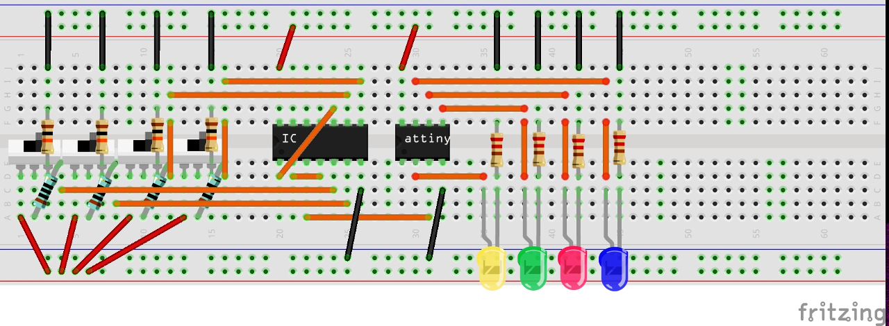
So assuming that we had an OR gate and an AND gate, we could program the scenario as follows.


6 2-way AND gates and 3 2-way OR gates showing Angus and Bertie with itchy fingers
But the blog title says "CD4011 NAND Logic Gate" so let's replace the AND/OR gates with the universal NAND gate.


6 2-way NAND gates, nobody pushing buttons
The purists out there (hi!) would instantly complain about uneven "propagation delays" in the diagram and fair enough too - thus we need to make sure that any path to launch is no shorter than any other, and so the final circuit has even paths as shown.

Even delays on each line, and Charlise trying to launch by herself
So let's build the circuit and then test it - to the bunker!


You might want to explore the boolean logic side of things a bit more, in which case I recommend this course from Stanford University and this one from the Hebrew University of Jerusalem.


Saturday, September 21, 2019

0000 0000 0000 1101

PS2501 Optocoupler

In the 21st century you don't need wires to transmit a signal, and in fact it might be dangerous to have two devices connected if there is a sudden surge either way. Also, maybe the voltage supply of your signalling device needs to be different or isolated from the voltage supply of your receiving device. Perhaps you hate signal noise and are looking to clean it up optically.

For whatever these reasons, you can use an optocoupler such as the PS2501 to bridge the gap between signal and receive as follows. This little device has an LED transmitter (1,2) and an NPN silicon phototransistor (3,4). The IC allows a signal transfer across an optical gap, with no physical connection between the circuits.


Hook up power on both sides and watch the...er...lack of connection?


Saturday, September 14, 2019

0000 0000 0000 1100

CD4077 XNOR Gate


For quite a long time the inspiration for buying electronics came primarily from online gurus such as Julian Illett, Big Clive, Great Scott and many others. If those enlightened souls reckoned an AP2112 3.3V regulator was a good thing then I jumped online and ordered a swag of them. It was great a couple of years ago because direct sourced components were cheap (and still remain relatively so compared to local suppliers), but of course I didn't really have the time or the talent to put these components to good use.

Then in 2018 I met young Joseph - a madcap toddler obsessed with repeatedly flicking on and off electrical outlet switches. He wasn't getting much joy from the flicking and it was driving his parents a little batty. I had a bit of think and dug around in the many buckets of components and came up with the idea of using an XNOR gate logic chip based circuit. 

The idea behind the CD4077 is that the state of the output pin ALWAYS changes when one of the input pins changes.


Pick a state, switch X or Y and watch Z change

Four inputs via buttons, and one output that will always change

The XNOR gate wired up with output from pin 3

Breadboarded for testing
Low skill soldering - but robust
So now code some randomness to confound the little tyke.

 1
 2
 3
 4
 5
 6
 7
 8
 9
10
11
12
13
14
15
16
17
18
19
20
21
22
23
24
25
26
27
28
29
30
31
32
33
34
35
36
37
38
39
40
41
42
43
44
45
46
47
48
49
50
51
52
53
54
55
56
57
58
59
60
61
62
63
64
65
66
67
68
69
70
// ATMEL ATTINY13a μC
// 
//                                   +-\/-+
//  RESET--ACD0--5/A0--PCINT5--PB5  1|    |8  VCC
//   CLKI--ACD3--3/A3--PCINT3--PB3  2|    |7  PB2--PCINT2--2/A1--SCK--ADC1
//         ACD2--4/A2--PCINT4--PB4  3|    |6  PB1--PCINT1---1---MISO--OCOB--INT0*
//                             GND  4|    |5  PB0--PCINT0---0---MOSI--OCOA*
//                                   +----+
//  * indicates PWM port

#include <avr/interrupt.h>                    // for interrupt routines
#include <avr/sleep.h>                        // the sleep routines

#define InterruptPin PB4                      // A2 interrupt pin
volatile uint16_t lastpins = 0b00000000;      // store last lights so they are not the same
volatile uint16_t whichpins = 0b00001111;     // storage for current lights
volatile uint16_t myrand = 2901;              // happy birthday

// generate a "random" number between small and big
uint16_t gimmerand(uint16_t small, uint16_t big) {
  myrand ^= (myrand << 13);
  myrand ^= (myrand >> 9);
  myrand ^= (myrand << 7);
  return abs(myrand)%23*(big-small)/23+small;
}

// gets a new set of random lights, then displays and stores them
void flickthem() {
  while (lastpins == whichpins) {
  whichpins = gimmerand(1, 15);
  }
  PORTB = whichpins;
  lastpins = whichpins;
  delay(50); 
}

// waits for button input, then grabs the new lights
void waitforswitch(void) {
    sei();                                // enable global interrupts
    set_sleep_mode(SLEEP_MODE_IDLE);      // sleep little one
    sleep_enable();                       // enable sleep mode
    sleep_mode();                         // system sleeps here
    
    sleep_disable();                      // ISR routine returns here so wake up        
    delay(50);                            // settle time

    flickthem();                          // change lights please
  
}

// Interrupt
ISR(PCINT0_vect)
{
  // wake up little one...
}

void setup() {
GIMSK |= (1<<PCIE);                   // activate Pin change interrupts
PCMSK |= (1<<InterruptPin);           // sets the Pin change interrupt mask
DDRB = 0b00000000;                    // make all Pins input
// read three pins and add for randomseed
myrand = analogRead(A0)+analogRead(A1)+analogRead(A2);
DDRB = 0b00001111;                    // set output pins for light
flickthem();                          // alive! all pins on to start with (setup check)
}

void loop() {
  // put your main code here, to run repeatedly:
  waitforswitch();                    // sleep and then wait for a button
}

and finally box the whole thing up and smother in hot glue!


Saturday, September 7, 2019

0000 0000 0000 1011

QX5252 Solar Light IC


Most electronics amateurs like myself are drawn to the "something for nothing" dark side of circuits via the "Joule Thief", a forgiving and interesting beast that looks a little like this in it's basic form.


By Rowland - Own work, CC BY-SA 3.0, https://commons.wikimedia.org/w/index.php?curid=31765405
I made up some little torches using this circuit with some hand wound ferrite cores (hours of fun watching TV and winding) and my favourite SS8050 as the NPN transistor (seen below in SOT-23 format on a little adapter board).


Bright little light using a "spent" AAA battery
I use this circuit also to grow succulents by harvesting the last of the "flat" batteries that come my way in little grow chambers like this one.


Tiny container with grow lights
A year or so ago I came across a link to a circuit based on the QX5252 chip. This little marvel is used extensively in your typical solar garden light, using a "joule thief" style circuit. 

They cost only a couple of cents each, but can easily be used to replace the transistor and some circuitry in the joule thief. You simply add an inductor (I'm exploring through hole radial inductors - no more late night winding) and presto you have a pretty robust circuit.

The next step was to make it stable enough if possible to run a microcontroller (μC) such as my favourite Attiny13. The output from the QX5252 might be good enough for an LED, but in fact the circuit oscillates and fools the human eye into believing that it is a steady light. The resultant signal oscillates too much for the μC.


Brighter minds have since come up with a way of stabilising the signal using the following components.


So now I can have a single AA or AAA NiMH or NiCad rechargeable battery happily running the μC at a much higher voltage using solar panel recharging - with the added bonus of protection built into the QX5252 for low voltage. I am still experimenting with the circuit by changing in and out the following:

    1. Other solar light ICs such as the YX805 or YX8018.
    2. Size and specs for the inductor (seems around 68μH is about right, a good trade when looking at efficiency vs current)
    3. Size and specs for the zener diode (at the moment hovering around 3-5V but still experimenting)
    4. Size and specs for the diode shown above as the 1N4007 (at the moment using 1N4148 both in through hole and SMD package format)

I've gone to EasyEDA and JLCPCB for little boards based on this circuit so watch this space for more development for these circuits. I like the idea of wringing a battery dry for both electronic reasons and also for environment reasons. It's my aim to have solar devices all over the house, powered at any voltage DC by the sun.


Just the "joule thief" QX5252 circuit in the design phase on EasyEDA

With the addition of the Attiny chip for the solar candle
I'm working on a breadboard friendly version where the μC has all the pins broken out to make it a bit more versatile.

Any 8-pin micro broken out for projects