CD4013 Flip Flop
In an earlier blog and video I was messing around with a fundamental element of computers, the Set/Reset Latch (S/R Latch), built around a CD4001 quad NOR gate. It's great, but evolution of this circuit has led to another element known as the S/R flip flop.
 |
| SR Latch |
 |
| SR Flip Flop |
There is SO MUCH information out there about these logic circuits, but I'll just recommend two sources if you are the type that likes to:
The fundamental change is that the SR Latch cannot change unless the Enable pin is HIGH (1). I also saw many Truth Tables out there and they were very inconsistent in their outputs of Q and Q' - depending on whether the Enable pin was also a Clock signal with a rising and falling edge. Interesting!
As a little side project I was wondering what the results would be if I replaced the AND gates with NOR gates!

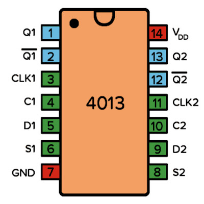
But ultimately I wanted to use the CD4013 IC, which is listed as a Dual D-Type Flip-Flop (the D being for Data). In the datasheet we see the following "function table":

And the pinout for the chip is as follows:
I think next I'll try the JK Flip Flop to avoid the "ambiguous" case which seems to be the downfall of this circuit.
No comments:
Post a Comment