CD4001/CD4081 Clocked D Flip Flop
I'm exploring CMOS chips and combinations of same. Recently I did a couple of circuits involving the CD4001 Quad 2-input NOR gate.
1. An SR Latch used as a car "indicator" circuit
2. An SR Latch for shutting down an entire circuit
The problem with an SR Latch is the so-called "illegal state" whereby the circuit cannot consolidate the signals into a cohesive output and some weird random oscillations take place.

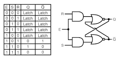

While mucking around with the simulator trying to figure out how this circuit works I decided to explore replacing the AND gates with NOR gates.
How could that work? See the video below

No comments:
Post a Comment